Physical Design is a process of transforming a circuit description into physical layout which describes the position of cells and routes for the interconnections between them. It is the result of a synthesized netlist that has been placed and routed. The design flow deals with various steps involved such as follows: Synthesized netlist ⇓ Partitioning ⇓ Sanity checks ⇓ Floorplan ⇓ Power plan ⇓ Placement ⇓ Clock Tree Structure (CTS) ⇓ Routing ⇓ Signoff Sanity checks has to be performed before every stage in order to check whether our design is meeting the requirements for the next stage (or) whether its properly designed. Basically, a code(program) is developed that explains us the RTL characteristics of the chip to be designed. That will be done by the front end engineers(RTL design team). The developed code is then compiled and as a result, a synthesized netlist is obtained. It contains the gate level model for the respective RTL code. .def is the output file at each s...
Scan chain is
detached and reordered without any change in functionality. It helps in
reducing congestion. Also helps in meeting timing and reducing IR drop as the
number of nets gets reduced.
Flops are converted into scan enabled flip flops and stitched into chains at
synthesis stage. It is done by DFT team.
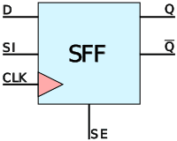 |
SEFF |
 |
Internal of SEFF |
 |
SEFF before Stitching |
- After reordering, the number of flops in the scan chain
should be same as before.
- First and last flops may change after reordering.
- Flops of different scan chains are exchanged and
reordered by considering partition. Partition is a group of "scandef
chains" that may exchange flops during reordering.
- Lockup latches and multiplexers breakup scan chains
further into "reordering buckets".

Comments
Post a Comment
Let us upgrade together. Please leave your comments for betterment