Physical Design is a process of transforming a circuit description into physical layout which describes the position of cells and routes for the interconnections between them. It is the result of a synthesized netlist that has been placed and routed. The design flow deals with various steps involved such as follows: Synthesized netlist ⇓ Partitioning ⇓ Sanity checks ⇓ Floorplan ⇓ Power plan ⇓ Placement ⇓ Clock Tree Structure (CTS) ⇓ Routing ⇓ Signoff Sanity checks has to be performed before every stage in order to check whether our design is meeting the requirements for the next stage (or) whether its properly designed. Basically, a code(program) is developed that explains us the RTL characteristics of the chip to be designed. That will be done by the front end engineers(RTL design team). The developed code is then compiled and as a result, a synthesized netlist is obtained. It contains the gate level model for the respective RTL code. .def is the output file at each s...
STA(Static Time Analysis):
It is the process of
analysing the timing constraints of the design without any
simulation/switching.
Basically, Timing
analysis is of 2 types.
1. STA - Static Timing
Analysis
2. DTA - Dynamic Timing
Analysis
Setup time: min. amount of time for which the data
signal is to be stable before the next active clock edge.
Hold time: min. amount of time for which the data
signal is to be stable after the first active clock edge.
Launch flop: flop that is responsible for launching the data.
Capture flop: flop that is responsible for capturing the data.
Launch clock: clock responsible for making launch flop active.
Capture clock: clock responsible for making capture flop active.
Launch time: time taken for launching the data.
Capture time: time taken for capturing the data.
Data path: path of data signal (or) path starting from common point of
clock network to the data pin of the capturing sequential cell.
Also called as
"launch path", "arrival time(AT)", "data arrival
time".
Clock path: path of clock signal (or) path sharing from common point of
clock network to the clock pin of capturing sequential cell.
Also called as
"capture path", "required time(RT)", "data required
time".
Critical path: timing path that fails to meet the timing constraints by
largest margin.
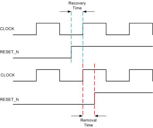
Recovery time: min. time that an asynchronous control input pin must
be stable before the next active clock edge. (or) min. amount of time between
release of an asynchronous signal from active state to next active clock edge.
Removal time: min. time that an asynchronous
control input pin must be stable after the first active clock edge.
(or) min. amount of time between active clock edge and release
of an asynchronous control signal.
For setup and hold analysis: Click here

Timing paths: The paths where the setup and hold analysis is to be done
(data paths) (or) the paths in which timing is to be calculated.
There are 7 types of
timing paths. Among these, 4 are mostly used. They are:
1. I2R - I/p to Register
2. R2O - Register to O/p
3. R2R - Register to
Register
4. I2O - I/p to O/p
The remaining three are:
5. I2M - I/p to Macro
(Memory)
6. M2O - Macro to O/p
7. M2M - Macro to Macro
Timing exceptions: The constraints that are not considered for
timing analysis.
1. False path:
physically existed but are logically/functionally inactive. It does not affect
the output and doesn't contribute to the delay of the circuit.
2. Multicycle
path: paths that require more than one clock cycle for its execution.
3. Min/max path
4. Disable
timing arcs: disabling the input to output arc.
Comments
Post a Comment
Let us upgrade together. Please leave your comments for betterment